UPDATES
IBS Center for Multidimensional Carbon Materials
Total : 62, Now : 2 page
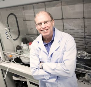
Dr. Rodney Ruoff delivers the ECS Lecture on May 31
The ECS Lecture at the Plenary Session of the 239th ECS Meeting with IMCS18 will be delivered by Dr. Rodney Ruoff, Distinguished Professor in the Departments of Chemistry and Materials Science, and the School of Energy Science and Chemical Engineering at the Ulsan National Institute of Science and Technology (UNIST), South Korea, and Director of the Center for Multidimensional Carbon Materials (CMCM). The Plenary Session is from 2100-2200h EST on Monday, May 31, after which the content will be available through June 26, 2021. The 239th ECS Meeting with IMCS18 takes place in a digital format. There is no cost to participate, however pre-registration is required.
ECS Lecture
For more than 50 years, notable leaders in the fields of electrochemistry and solid state science—including numerous Nobel Laureates—have presented the ECS Lecture. In his presentation, “Carbon Materials,” Dr. Ruoff discusses the intimate connection between …
작성자 : CMCM
2021.05.25
그래핀 합성 시간 단축할 실마리 찾았다
韓-中연구진, 컴퓨터 시뮬레이션으로 그래핀 합성 과정 규명
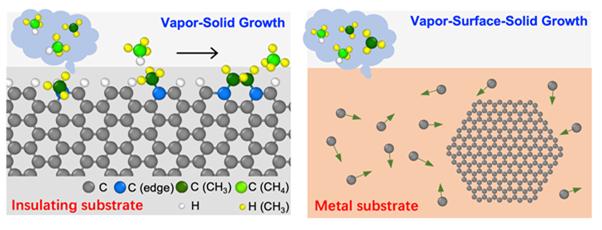
그래핀을 전자소자로 활용하려면 기판 위에서 그래핀을 합성한 뒤, 분리해내는 공정이 필요하다. 이때 그래핀이 손상되기 쉬울뿐더러 분리 공정 자체도 까다롭다. 전자소자 재료 위에서 곧바로 그래핀을 합성하면 간단하지만, 합성 시간이 오래 걸린다는 문제가 있다. 한국과 중국 공동연구진이 이 문제를 해결할 단서를 발견했다.
▲ 그래핀은 탄소 원자 6개로 된 육각형 고리가 이어 붙은 2차원 물질이다. 강철보다 강하면서도 유연하고 투명하며, 전기전도성 또한 전선 소재로 쓰는 구리보다 100배 이상 좋다. 이 때문에 반도체 소자 집적 한계를 돌파할 새로운 반도체 재료로 각광받는다. (출처: Flickr)
기초과학연구원(IBS) 다차원 탄소재료 연구단 펑딩 그룹리더(UNIST 신소재공학과 특훈교수) 연구팀은 중국 베이징대와 공동으로 그래핀의 합성속도가 금속 기판보다 실리콘과 같은 절연체 위에서 1만 배 이상 느려지는 원인을 규명했다.
그래핀은 탄소(C) 원자 6개로 된 육각형 고리가 이어 붙은 2차원 물질이다. 고품질 그래핀 합성에는 주로 화학기상증착법(CVD)이 쓰인다. 기판 위에 메탄(CH4) 등 원료 기체를 주입하면, 탄소 원자가 기판에 흡착하며 하나 둘씩 붙어 그래핀이 성장하게 된다. 이때 사용되는 기판에 따라 그래핀 성장속도에 차이가 있지만, 아직까지 그 메커니즘이 명확히 밝혀지지는 않았다.
공동연구진은 컴퓨터 시뮬레이션을 통해 그래핀 합성 단계를 분석한 결과, 절연체와 금속 기판 위에서 그래핀 성장 과정에 차이가 있음을 발견했다. 절연체 기판을 쓸 때는 원료가 그래핀 가장자리에 달라붙는 방식으로 성장한다. 이 경우 수소가 함께 붙게 되는데, 수소 제거에 많은 에너지가 소모돼 성장이 느리다. 반면, 금속 기판을 쓰면 원료가 금속 기판을 타고 빠르게 이동할 수 있어 그래핀 성장이 빠르다.
▲ 절연체 기판(왼쪽) 위…
작성자 : CMCM
2021.04.26
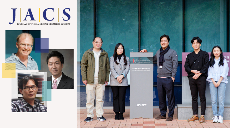
The synergy between IBS and UNIST propels research forward
In addition to its headquarters in Daejeon, IBS is operating campus research centers at various universities, including five universities specializing in science and technology. This enables researchers to freely engage in research projects under creative topics of their choice and collaborate with one another without the pressure of meeting deadlines. Among them, Ulsan National Institute of Science and Technology (UNIST) is home to three IBS research centers in three different fields that are generating world-class outcomes in basic science research. IBS Research met and heard from researchers who serve as a link between IBS and UNIST about the synergy they have been creating.
“The cooperation between IBS and UNIST helps us remain open to all ideas and march towards a common goal together.”
“I have engaged in many joint research projects with researchers from various fields since my years in the US, but working at…
작성자 : CMCM
2021.01.20
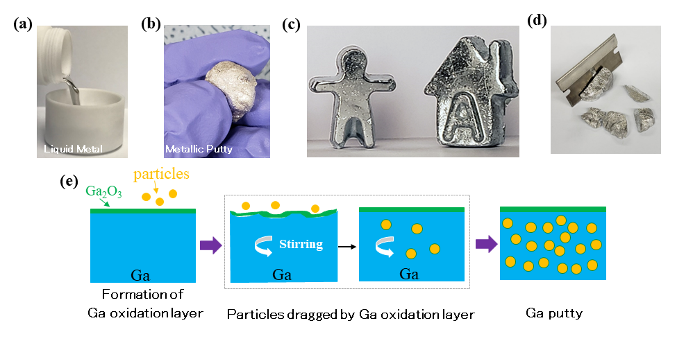
Putty-like composites of gallium metal with potential for real-world application
- Excellent intrinsic properties of these composites will allow them to have a wide range of use, from shielding the grid from coronal mass ejection events to more effective thermal pastes -
Gallium is a highly useful element that has accompanied the advancement of human civilization throughout the 20th century. Gallium is designated as a technologically critical element, as it is essential for the fabrication of semiconductors and transistors. Notably, gallium nitride and related compounds allowed for the discovery of the blue LED, which was the final key in the development of an energy-efficient and long-lasting white LED lighting system. This discovery has led to the awarding of the 2014 Nobel Prize in Physics. It is estimated that up to 98% of the demand for gallium originates from the semiconductor and electronics industry.
In addition to its use in electronics, the unique physical properties…
작성자 : CMCM
2021.01.09

IBS 과학자 7명, 피인용 세계 상위 1% 연구자(HCR)로 선정
- 국내 HCR 41명 발표…로드니 루오프·현택환 단장 7년 연속 선정 -
올해 세계에서 가장 영향력 있는 연구를 펼친 연구자 명단에 기초과학연구원(IBS, 원장 노도영) 소속 7명의 연구자가 이름을 올렸다.
글로벌 학술정보서비스 분석기업 클래리베이트 애널리틱스(이하 클래리베이트)가 18일 발표한 ‘2020 피인용 세계 상위 1% 연구자(Highly Cited Researcher ·HCR)’에 따르면 2020년 국내 HCR 41명(중복분야 포함 46명) 중 IBS 소속 연구자는 7명(중복분야 포함 9명)으로 확인됐다. 국내 연구기관 및 대학 중에서는 서울대(8명)에 이어 두 번째로 많은 숫자다.
클래리베이트가 HCR를 선정한 건 올해로 7년째다. 최근 11년간 피인용 횟수가 상위 1%에 해당하는 논문(Highly Cited Papers)을 발표하고, 동료 연구자들에게 중요한 영향을 미친 연구자들이 HCR로 선정된다. 올해는 전 세계 60여 개국 총 6,167명의 연구자가 HCR로 선정됐다.
로드니 루오프 단장(다차원 탄소재료 연구단)과 현택환 단장(나노입자 연구단)은 화학과 재료과학의 2개 분야에 선정되며 7년 연속(2014~2020년) HCR 명단에 이름을 올렸다.
이 외에도 장석복 단장(분자활성 촉매반응 연구단‧화학)은 6년 연속(2015~2020년), 김진수 수석연구위원(유전체 교정 연구단·생물학 및 생화학), 이영희 단장(나노구조물리 연구단·크로스 필드), 악셀 팀머만 단장(기후물리 연구단·환경 및 생태학), 김대형 부연구단장(나노입자 연구단·재료과학)은 3년 연속 HCR로 선정됐다.
현재까지 총 11명의 IBS 소속 연구자가 HCR로 선정됐다. 노도영 원장은 “IBS 연구자들이 영향력 높은 연구로 국제적으로 인정받고 있다는 의미”라며 “HCR을 비롯한 IBS의 우수한 연구진의 도전이 더욱 날개를 펼칠 수 있도록 뒷받침하겠다”고 말했다.
…
작성자 : CMCM
2020.11.27
Oxygen can do a favor to synthesize metal-organic frameworks
Metal-organic frameworks, or MOFs, are composed of metal ions periodically surrounded by organic bridging molecules, and these hybrid crystalline frameworks feature a cage-like hollow structure. This unique structure motif offers great potential for a range of applications in energy storage, chemical transformations, optoelectronics, chemiresistive sensing, and (photo)electrocatalysis, among others. Debuted in the early 2000s, MOFs are a fascinating nanomaterial. Though numerous applications exploit MOFs, little has been known as to how oxygen may work in the synthesis of MOFs.
Led by Director Rodney S. Ruoff and senior chemist Dr. Yi Jiang, chemists from the Center for Multidimensional Carbon Materials (CMCM) within the Institute for Basic Science (IBS) located at Ulsan National Institute of Science and Technology (UNIST) in collaboration with their colleagues at UNIST and Sungkyunkwan University (SKKU) have identif…
작성자 : CMCM
2020.10.27