UPDATES
IBS Center for Multidimensional Carbon Materials
Total : 61, Now : 3 page
반도체 칩 안에 금속 배선을 분리하는 새로운 소재가 개발됐다. 이 소재를 이용하면 소자를 아주 작게 만들 수 있고, 메모리와 같은 반도체 칩의 작동 속도를 높일 수 있다.
UNIST(총장 이용훈) 자연과학부의 신현석 교수팀과 삼성전자 종합기술원(원장 황성우)의 신현진 전문연구원팀, 기초과학연구원(IBS)을 포함하는 국제 공동 연구진이 반도체 집적회로(Integrated Chip, IC칩)에 사용될 수 있는 ‘초저유전율 절연체’를 개발했다. 합성된 절연체를 사용하면 반도체 회로 간 전기적 간섭을 획기적으로 줄여 ‘소자 미세화’가 가능하다.
반도체 칩에 많은 데이터를 저장하고 정보처리 속도를 빠르게 하려면, 칩 안에 소자 숫자가 늘어나야 한다. 하지만 더 많은 소자를 넣으려고 소자 크기를 작게 만들면 오히려 정보처리 속도가 느려질 수 있다. 반도체 내부에서 전자를 금속 배선 안에만 머무르게 만드는 ‘절연체’가 전자를 모으는 성질(유전율)이 있어 전자의 흐름을 방해하기 때문이다. 반도체 소자가 작아지고 배선 사이 간격이 좁아지면 이러한 현상이 더 심해진다. 따라서 반도체 소자의 집적도를 높이려면, 금속 배선에서 전자 이탈은 막으면서도 유전율은 낮은 절연체가 필요하다.
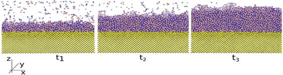
그림1. 비정질 질화붕소 증착과정
공동 연구팀은 기존 절연체보다 낮은 유전율을 갖는 ‘비정질 질화붕소(amorphous boron nitride) 소재’를 합성하고, 낮은 유전율을 갖는 원인을 밝혀냈다. 원래 질화붕소는 다양한 결정이 존재하는데, 화이트 그래핀으로 알려진 육방정계 질화붕소는 그래핀같이 육각형의 규칙적인 원자 배치이지만 이번에 합성된 질화붕소는 원자 배치가 불규칙한 ‘비정질’이다. 합성된 물질의 유전율은 1.78로 현재 사용되는 절연체의 유전율보다 30% 이상 낮다.
그림 2. 비정질 질화붕소의 성질. 금속 확산 방지막 역할도 수행한다.
제1저자인 홍석모 UNIST 자연과학부 박사과정 연구원은 “낮은 온도(400℃)에서 육방정계 질화붕소가 기판에 증착되는지 연구…
작성자 : CMCM
2020.07.07
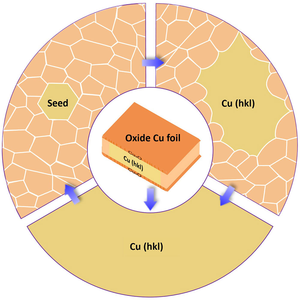
Tuning the Surface Gives Variations to Metal Foils
A4 paper-sized single-crystal metal foils with various surface structures are obtained by seeded annealing
Just as cloning in biology allows for the creation of one or more replicas of the exact same genes, seeded growth in chemistry can produce a very large metal foil with the exact same surface texture as that of a seeded one. Seeded growth is very popular in synthesizing three-dimensional (3D) single crystals: 3D crystals are always grown into the same shapes, just as salts are invariably cubic single crystals.
Meanwhile, very thin foils/films can grow into different types depending on surface structures. As such, applications can vary. Great efforts had been dedicated to the synthesis of single crystalline metal foils as they have many important applications, such as (i) a substrate to support the synthesis of various two-dimensional (2D) materials, (ii) engineering the properties of the material deposited on it, (iii) allo…
작성자 : CMCM
2020.06.03

■ 로드니 루오프 교수, 마이크로소프트 아카데믹 재료과학 부문 전체 2위 올라!
로드니 루오프(Rodney S, Ruoff) 자연과학부 특훈교수(IBS 다차원탄소재료연구단장)이 ‘마이크로소프트 아카데믹(Microsoft Academic)’의 재료과학(Materials Science) 부문에서 전체 2위의 우수 저자(Top Author)로 이름을 올렸습니다.
루오프 교수는 ‘중요성(Saliency)’ 부문과 ‘피인용(Citation)’ 부문에서 모두 2위에 이름을 올렸는데요. 관련 분야에 영향력 있는 연구를 꾸준히 배출해 온 성과입니다. 그는 UNIST 학내에서도 1소속인 자연과학부 화학과는 물론 신소재공학부, 에너지 및 화학공학부와의 활발한 공동 연구를 통해 우수한 성과를 다수 선보이고 있습니다.
한편 마이크로소프트 아카데믹은 마이크로소프트의 학술 데이터베이스를 바탕으로 제작된 학술 검색 엔진으로, 다양한 학술저작과 저자들, 저널, 기관과 각 주제별 분류 데이터를 제공하고 있습니다.
@Post credit to UNIST, see original post HERE @Go Microsoft Academic
작성자 : CMCM
2020.05.20
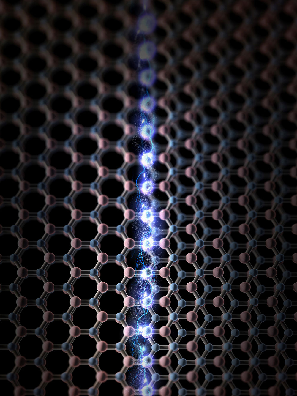
An ultimate one-dimensional electronic channel in hexagonal boron nitride
- A zero bandgap boundary discovered in insulating hexagonal boron nitride sheets with could pave the way for new nano-electronic devices -
In the field of 2D electronics, the norm used to be that graphene is the main protagonist and hexagonal boron nitride (hBN) is its insulating passive support. Researchers of the Center for Multidimensional Carbon Materials (CMCM) within the Institute for Basic Science (IBS, South Korea) made a discovery that might change the role of hBN. They have reported that stacking of ultrathin sheets of hBN in a particular way creates a conducting boundary with zero bandgap. In other words, the same material could block the flow of electrons, as a good insulator, and also conduct electricity in a specific location. Published in the journal Science Advances, this result is expected to raise interest in hBN by giving it a more active part in 2D electronics.
Similarly to graphene, …
작성자 : CMCM
2020.03.09
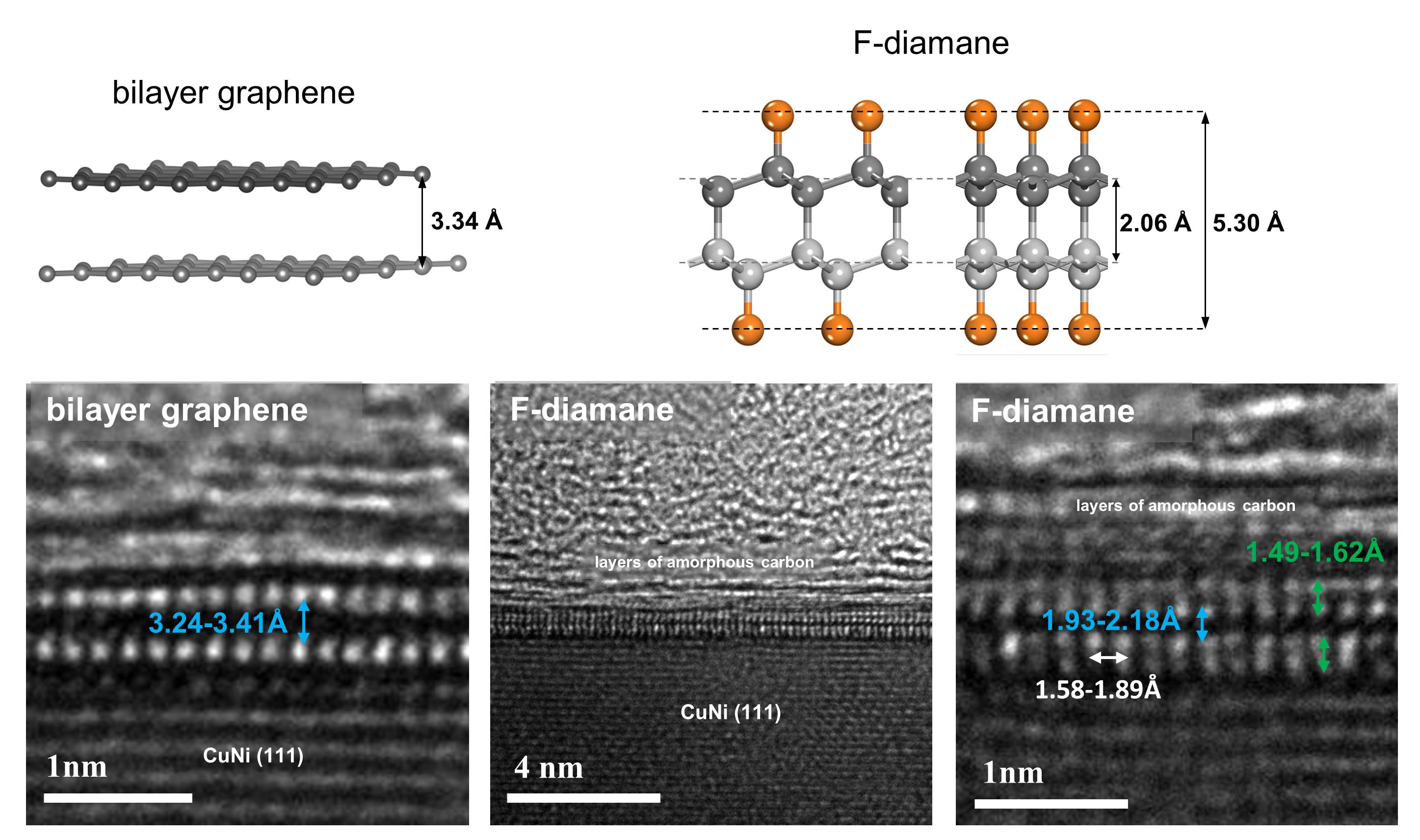
Research published in Nature Nanotechnology shows that diamond and graphite are just a few chemical reactions apart. A research team led by Rodney S. Ruoff of Ulsan National Institute of Science and Technology in South Korea has demonstrated conversion of large-area bilayer graphene to F-diamane—an ultrathin, fluorinated diamond-like material—under non-extreme temperature and pressure conditions upon fluorination.
“The conversion from bilayer AB-stacked graphene to the thinnest possible diamond-like material is indeed possible without using extreme conditions, like high pressure,” says Pavel Bakharev, a research fellow in physics at the Center for Multidimensional Carbon Materials (CMCM) at the Institute for Basic Science in Ulsan, South Korea, and lead author of the findings. “[There have been] multiple theoretical papers on this conversion, but until now, it [has never been shown] experimentally.”
(Top): Optimized models of bilayer graphene and fluorinated monolayer diamond (…
작성자 : CMCM
2020.01.28

A tech jewel: Converting graphene into diamond film
- Synthesis of the thinnest possible diamond-like material starting from bilayer graphene and without high pressure -
Can two layers of the “king of the wonder materials,” i.e. graphene, be linked and converted to the thinnest diamond-like material, the “king of the crystals”? Researchers of the Center for Multidimensional Carbon Materials (CMCM) within the Institute for Basic Science (IBS, South Korea) have reported in Nature Nanotechnology the first experimental observation of a chemically induced conversion of large-area bilayer graphene to the thinnest possible diamond-like material, under moderate pressure and temperature conditions. This flexible, strong material is a wide-band gap semiconductor, and thus has potential for industrial applications in nano-optics, nanoelectronics, and can serve as a promising platform for micro- and nano-electromechanical systems.
Diamond, pencil lead, and graphene are made by the same bu…
작성자 : CMCM
2019.12.11