UPDATES
IBS Center for Multidimensional Carbon Materials
11 Oct 2018 /
CMCM
The image editing credit goes to UNIST
New Study Reveals Fast Growth
of Highly-Oriented Monolayer Graphene on a Cu/Ni(111) Alloy Foil
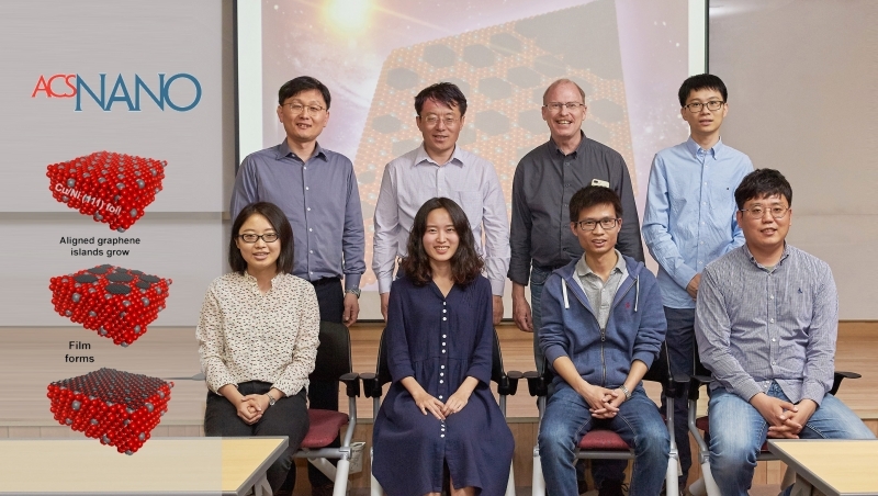
An international research team, affiliated with UNIST announced that they had succeeded in achieving the fast growth of near single crystal monolayer graphene on homemade single crystal Cu/Ni(111) metal foils. The result has greatly accelerated the growth of graphene — at least ten times faster than the previous record, according to the research team.
This breakthrough has been led by Distinguished Professor Rodney S. Ruoff and his research group from the Center for Multidimensional Carbon Materials (CMCM), within the Institute for Basic Science (IBS) at UNIST.
This breakthrough has been led by Distinguished Professor Rodney S. Ruoff and his research group from the Center for Multidimensional Carbon Materials (CMCM), within the Institute for Basic Science (IBS) at UNIST.
Chemical vapor deposition (CVD) is currently the most versatile and promising method for graphene growth and it employs polycrystalline Cu foil as a catalystic substrate. Under the flow of methane (CH4) and hydrogen (H2) gas mixture, synthesis of graphene is carried out on Cu substrates. Since the crystal orientation of the underlying Cu substrates varies, graphene domains growing on such a polycrystalline surface cannot exclude the influence of the underlying Cu substrates.
Chemical vapor deposition (CVD) is currently the most versatile and promising method for graphene growth and it employs polycrystalline Cu foil as a catalystic substrate. Under the flow of methane (CH4) and hydrogen (H2) gas mixture, synthesis of graphene is carried out on Cu substrates. Since the crystal orientation of the underlying Cu substrates varies, graphene domains growing on such a polycrystalline surface cannot exclude the influence of the underlying Cu substrates.
However, the polycrystalline nature of CVD graphene grown on Cu can be a problem for graphene-based devices because it may degrade the exceptional electonic properties and charge transport in graphene. Scientists have been searching for ways to achieve highly oriented single-crystal monolayer graphene, thereby makeingfull use of exceptional properties of graphene.
However, the polycrystalline nature of CVD graphene grown on Cu can be a problem for graphene-based devices because it may degrade the exceptional electonic properties and charge transport in graphene. Scientists have been searching for ways to achieve highly oriented single-crystal monolayer graphene, thereby makeingfull use of exceptional properties of graphene.
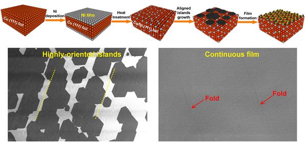
Making the Cu/Ni(111) alloy foil and the typical growth of highly oriented single-layer graphene.
“Compared with Cu foils used for graphene growth, the Cu/Ni(111) foils, in the range of composition from 1.3 at.% to 8.6 at.% Ni, promote the fast growth of a full coverage of near single-crystal graphene film in only 5 minutes (as compared to 60 minutes for a pure Cu(111) foil),” says Ming Huang in the Combined M.S./Ph.D. of Materials Science and Engineering, the co-author of the study.
“Compared with Cu foils used for graphene growth, the Cu/Ni(111) foils, in the range of composition from 1.3 at.% to 8.6 at.% Ni, promote the fast growth of a full coverage of near single-crystal graphene film in only 5 minutes (as compared to 60 minutes for a pure Cu(111) foil),” says Ming Huang in the Combined M.S./Ph.D. of Materials Science and Engineering, the co-author of the study.
This is explained by the enhanced growth rate of graphene on the Cu/Ni(111) surface. “The measured rates of graphene island growth show that inserting Ni atoms in the Cu(111) foil surface significantly reduces the energy barriers to the decomposition of methane and dramatically increases the rate of growth (by DFT calculations)”, said coauthor Mandakini Biswal.
This is explained by the enhanced growth rate of graphene on the Cu/Ni(111) surface. “The measured rates of graphene island growth show that inserting Ni atoms in the Cu(111) foil surface significantly reduces the energy barriers to the decomposition of methane and dramatically increases the rate of growth (by DFT calculations)”, said coauthor Mandakini Biswal.
Experimentally measured rates were supported by theoretical calculations of the decomposition of methane molecules.
Experimentally measured rates were supported by theoretical calculations of the decomposition of methane molecules.
Coauthor Lu Qiu noted that “all of the energy barriers for decomposing CH4 into CHi (i = 3, 2, 1, 0) in sequence are greatly reduced; for example, the energy barrier for decomposing a CH4 molecule to a CH3 radical on Cu(111) is 1.56 eV, whereas it is only 0.88 eV on this Cu/Ni(111) surface. The reduction of the energy barrier (0.68 eV) will greatly accelerate the CH4 dissociation on the Cu/Ni(111) surface.”
Coauthor Lu Qiu noted that “all of the energy barriers for decomposing CH4 into CHi (i = 3, 2, 1, 0) in sequence are greatly reduced; for example, the energy barrier for decomposing a CH4 molecule to a CH3 radical on Cu(111) is 1.56 eV, whereas it is only 0.88 eV on this Cu/Ni(111) surface. The reduction of the energy barrier (0.68 eV) will greatly accelerate the CH4 dissociation on the Cu/Ni(111) surface.”
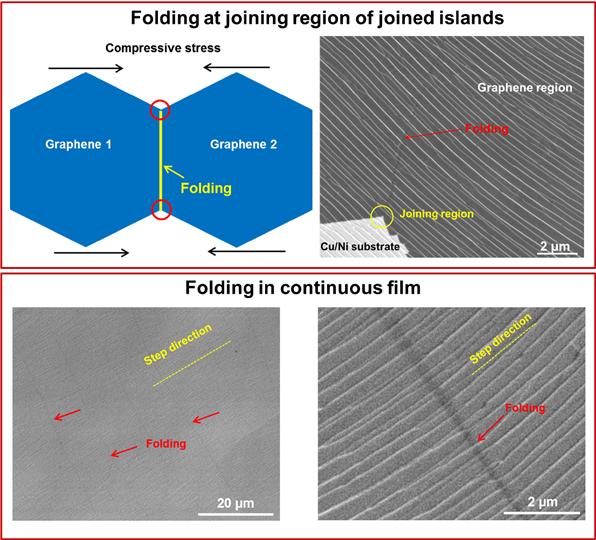
Folding in joined graphene islands and continuous graphene film.
“We discovered, by using low energy electron diffraction (LEED) that the surface of the Cu/Ni(111) foil does not have a random distribution of Ni but instead has a superstructure (a layer only one or two atoms thick) with composition Cu6Ni1,” said coauthor Hyunseob Lim. This Cu6Ni1 surface superstructure is present for at least the composition range from 1.3 to 7.8 bulk at.%, and this was discovered by preparing and doing LEED on foils with (specifically) the bulk atomic percentage of Ni of 1.3, 2.4, 3.9, 5.9, 6.2, and 7.8 at.% Ni.
Coauthor Da Luo notes “the continuous single crystal graphene has folded regions millimeters in length that are roughly 40 nm wide (they can be as wide as 300 nm) spaced by roughly 20 µm that run more or less parallel to each other and are always perpendicular to step edges in the metal foil surface.” Coauthor Hyo Ju Park said “apart from these parallel folds in continuous film, folds are also observed at the ‘join regions’ of joined graphene islands (obtained by deliberate incomplete growth runs).
We first observed these by high resolution transmission electron microscopy.” Ruoff explains: “These folds are due to the release of compressive stress (stress concentration occurs in these joining regions), but in a different way than for the continuous films. All published papers to date have not identified the presence of such folds in either continuous films on single crystal substrates where this significant thermal contraction of the substrate happens, or for joined islands on the same types of substrates.”
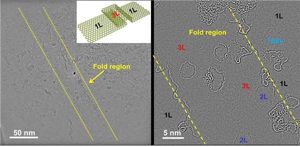
TEM images with different magnifications showing the folding structure (3- layer structure) at the joining region of two joined graphene islands. 1L is the monolayer graphene region, 3L is the folded region and the 2L region (etched 3L region) is due to the e-beam irradiation of the 3L region.
“This is the first report of single crystal Cu/Ni(111) foils, the first report of a superstructure of Ni in the Cu lattice in the top atomic layer(s) in a Cu/Ni(111) crystal, the first report of such exceptionally fast growth of epitaxial graphene on a metal foil surface and the first study of such 3-layer thick fold regions,” says Professor Ruoff.
“This study of graphene islands joining (that eventually form a continuous film) provides a methodology that will benefit the study of the joining of islands in other 2D materials and thin films,” Biswal notes.
“This study of graphene islands joining (that eventually form a continuous film) provides a methodology that will benefit the study of the joining of islands in other 2D materials and thin films,” Biswal notes.
This research was supported by the Institute for Basic Science and has been published in the journal, ACS Nano on May 23, 2018.
This research was supported by the Institute for Basic Science and has been published in the journal, ACS Nano on May 23, 2018.
Journal Reference
Journal Reference
Ming Huang et. al., “Highly Oriented Monolayer Graphene Grown on a Cu/Ni(111) Alloy Foil” ACS Nano, (2018).
*Article credit goes to UNIST, published on May 27, 2018